|
Turn your EasyPic2 development board into an
ENC28J60 Ethernet Toolkit
 This page will show you
how to connect your development board to the Ethernet Network, using the
ENC28J60 Microchip Ethernet Controller. This page will show you
how to connect your development board to the Ethernet Network, using the
ENC28J60 Microchip Ethernet Controller.
You will be surprised to see how simple it
is !
The
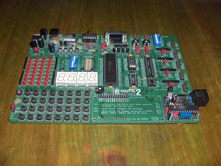
EasyPic2 : A good candidate for this enhancement
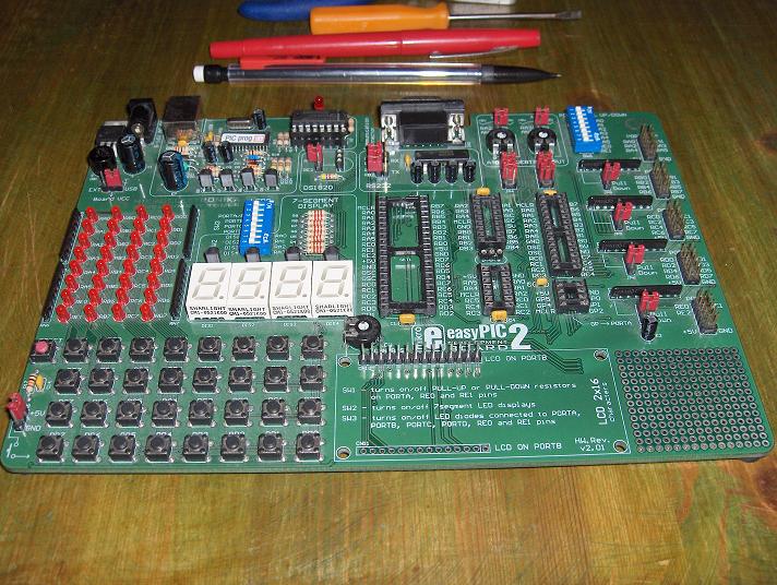
This is my good old EasyPic2 development board from
MikroElektronika. This is the one
I
fried one day... But it is still healthy and does
a lot of good job. For those who don't know this board, here is a little review
of its main features :
-
On-board USB fast programmer
-
DIP8 to DIP40 PIC sockets
-
32 LEDs and 32 buttons, connected to I/O
pins
-
4 digits 7 segments LED display
-
Socket for 2x16 LCD text display
-
2 trimmers for A/D conversion
-
5 connectors, directly connected to I/O pins
with pull-up/pull-down resistor arrays
-
RS232 adaptor and
connector
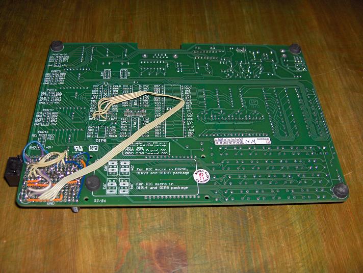
What do we see bottom right ? Let's have a look
closer...
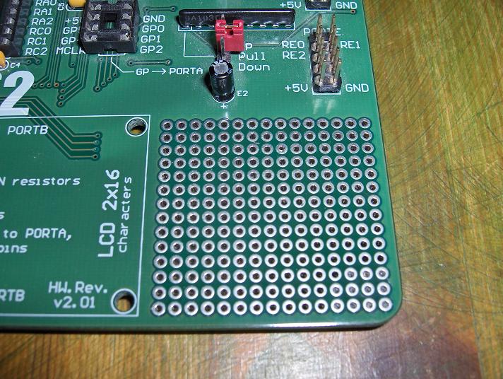
There was space left on the board, so
MikroElektronika had the good idea to make a prototype area for users.
210
plated-trough holes, both sides solder mask : until this day I never used this
area.
On the back side, we see that the upper row is
connected to the +5V power line, and the lower row to the ground
line.
Good ! Nature hates empty spaces isn't it ?
Me too !
What do we need ?
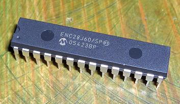
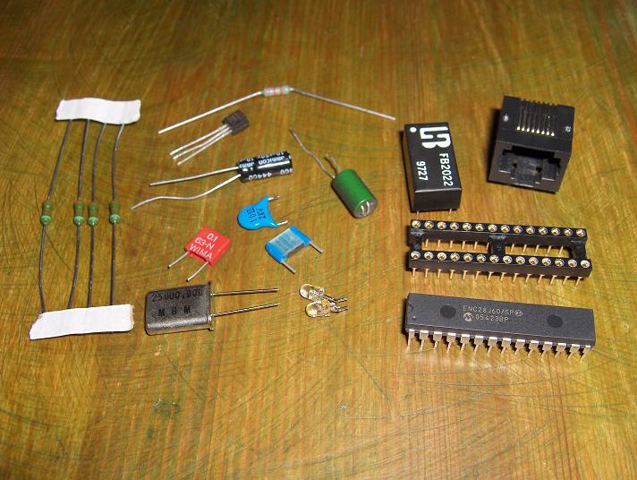 Almost all that you need is on this picture. The heart of the
circuit is the ENC28J60 Microchip Serial Ethernet Adapter, it is now widely
available, and its DIP28 package is very convenient for prototyping. Almost all that you need is on this picture. The heart of the
circuit is the ENC28J60 Microchip Serial Ethernet Adapter, it is now widely
available, and its DIP28 package is very convenient for prototyping.
Other
important part is the 3.3V voltage regulator (transistor-like 3-pins plastic
case on the picture) : the ENC28J60 can't operate directly with the +5V provided
by the board.
The 25 Mhz crystal for ENC28J60 clock is easy to find at
your usual supplier.
You will have also to find a magnetic for ethernet
network (black rectangular box left to the RJ-45 socket), this one comes from an
old ethernet hub board, as well as other parts seen on this picture. There are
now RJ-45 sockets with integrated LEDs and magnetic, if you want to save more
space on your board.
And now, go shopping :
| Quantity |
Part # or value |
Type |
| 1 |
ENC28J60 (Microchip) |
Serial Ethernet Controller |
| 1 |
LP2950CZ-3.3 |
+3.3V voltage regulator |
| 1 |
25 MHz |
crystal |
| 1 |
Green |
LED |
| 1 |
Red |
LED |
| 1 |
10 µF 25V |
capacitor |
| 1 |
47 µF 25V |
capacitor |
| 2 |
10 nF |
capacitor |
| 2 |
15 pF |
capacitor |
| 1 |
100 nF |
capacitor |
| 1 |
1 nF 2KV |
capacitor |
| 4 |
50 Ohm 1% |
precision resistor |
| 1 |
2.7 K 1% |
precision resistor |
| 2 |
470 Ohm |
resistor |
| 1 |
FB2022 |
TX/RX magnetic filter |
| 1 |
ferrite bead (value not critical) |
inductor |
| 1 |
DIP 28 pins |
IC socket |
| 1 |
RJ45 |
female solderable socket |
| 1 |
2x5 pins connector + 5 jumpers |
used as switch |
The circuit schematic
The circuit schematic comes from the datasheet of the ENC28J60 :
http://ww1.microchip.com/downloads/en/DeviceDoc/39662a.pdf
and
its errata :
http://ww1.microchip.com/downloads/en/DeviceDoc/80257a.pdf
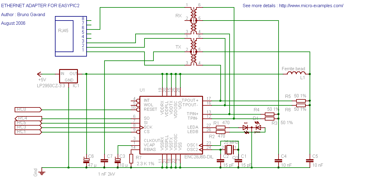
Click on the picture to enlarge the schematic
Please note that pin assignement of the TX/RX filter is not correct on
this schematic due to lack of library for FB2022 transformer. You will have to
refer to the datasheet of the part you will use (here is FB2022 datasheet)
As you can see, it is pretty simple :
The ENC controller is connected to
the network through a magnetic adapter.
It needs a 25 Mhz crystal for its
internal clock, resistors & capacitors for terminations, a 2.7K bias
resistor, and a 10 µF capacitor to stabilize its internal 2.5V power
supply.
The controller can directly drive two programmable LEDs through
current limitation resistors.
It is connected to the PIC through a
5 lines bus : reset line (RESET), chip select line (CS), SPI clock (CLK),
SPI data input (SI), SPI data output (S0).
There are also 2 control lines
that are not used in this exemple, but you can add them if you want, they are
the interrupt line (INT) and the wake up on lan line (WOL). They can be used to
trigger PIC interrupts, but in this example we operate using the polling method
and we don't need them.
The most frequently asked question about this controler is the voltage level
adaptation. The controller operates at 3.3V and the PIC on the board operates at
5.0V.
So, the question is : how to adapt ENC voltage levels to PIC voltage
level ?
We must consider both sides :
PIC output voltage for logical 1 is 5V :
does ENC accepts 5V on its inputs, whereas it is 3.3V powered ?
The answer is
yes, ENC inputs are 5V compliant, so that there is no risk for the controller to
apply 5V on its inputs, and they will correspond to logical
1.
ENC output voltage for logical 1 is 3.3V
: will the inputs of the PIC turn high or low when 3.3V coming from the ENC
outputs is applied ?
The answer is : it depends on the inputs of the
PIC. TTL inputs give logical 1 above 2.05V, and will not require voltage level
shifting. Schmitt trigger inputs give logical 1 above 3.5V, and will require
voltage level shifting.
In fact, we can consider that if we connect ENC outputs to PIC TTL inputs
only, the voltage level adapter is... a wire.
Most of PICs have TTL inputs
and integrated SPI on PORTC, so we will connect all ENC line to this port.
Assembly
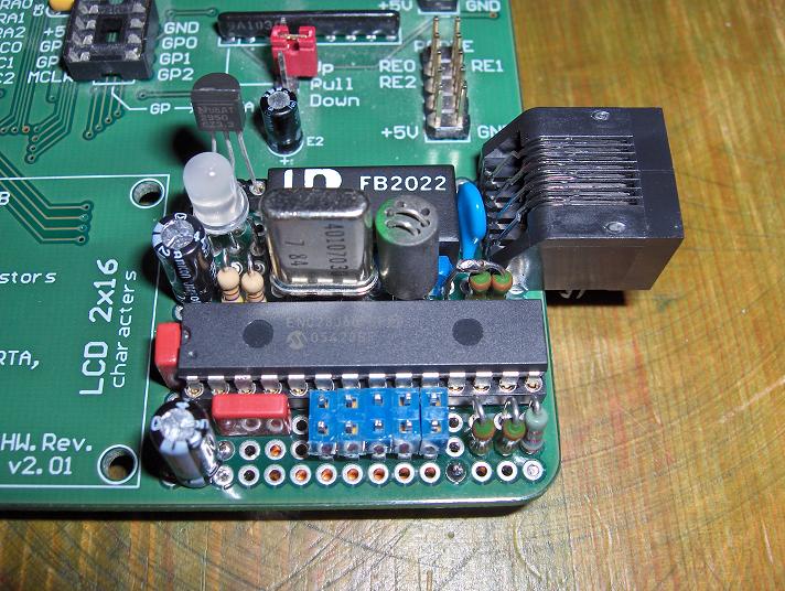
After soldering, you should get something that looks like this
:
As you can see, I used a red/green bicolor LED instead of the two
LEDs.
The jumper socket is placed just in front of the five lines that
are connected to the PIC, so that removing the jumper isolates the ethernet
circuit from the PIC, and PORTC can be used for other purposes.
The 3.3V regulator is mounted on a tulip socket : I have
only one for now, and it is shared with another test board.
The 25 Mhz crystal is also mounted on a tulip socket, to save
place for the two 15 pF capacitors hidden behind.
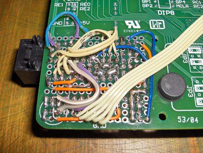
I'm a little bit ashamed, but I show you the back side anyway.
Sorry for the mess ;-)
Take care to respect the receive circuit polarity, because ENC is not able to
detect it correctly due to a silicon bug. That's why I used color wires. If you
connect it wrong, you may either have receive problem, or no receive at all.
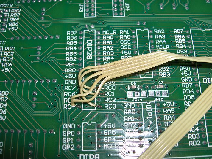
The bus is connected to the PORTC pins of the DIP28 socket.
Note that my cable deserves to be shortened...
Finally, this is what it looks like :
| Front side |
Back side |
 |
 |
And now...
Testing the ethernet board with a source
code example
It's time !
First, check and double-check all connections.
Don't plug the ENC28J60 in
its socket, then power the board and verify the 3.3V power supply on each pin of
the ENC.
Then turn the board off, put a 40 pins PIC as a PIC16F877A or a PIC18F452 in
its socket, and clock it at its maximum speed.
Plug the ENC28J60 in its
socket, and set the fiver jumpers to enable bus line between PIC and ENC.
Copy this mikroC source code and paste it in the mikroC compiler editor. If
you don't have this PIC compiler already, download it for free
now :
http://www.mikroe.com/en/compilers/mikroc/pic/download.htm
/*
 * file         : ep2enc28j60demo.c
 * project      : Ethernet controller ENC28J60 SPI communication test file
 * author       : Bruno Gavand
 * compiler     : mikroC V5.0.0.3
 * date         : july 26 2006
 *
 * description  :
 *      this code sets LEDA as link status display
 *      and makes LEDB blink permamently
 *
 * target devices :
 *      any PIC with integrated SPI on PORTC
 *      38 to 40 MHz clock is recommended to get from 8 to 10 Mhz SPI clock,
 *      otherwise PIC should be clocked by ENC clock output due to ENC silicon bug in SPI hardware
 *      tested with PIC16F877A@10Mhz, PIC18F452@40Mhz
 *
 *
 * EP2 settings :
 *      PORTC : pull-down
 *
 *      RC0 : !RESET    to ENC reset input pin
 *      RC1 : !CS       to ENC chip select input pin
 *      the ENC28J60 SPI bus CLK, SO, SI must be connected to the corresponding SPI pins of the PIC
 *      the INT and WOL signals from the ENC are not used
 *
 * see more details on http://www.micro-examples.com/
 *
 */

/*
 *  ENC SPI commands
 */
#define WCRCMD  0b01000000      // write control register
#define BFCCMD  0b10100000      // bit field clear
#define BFSCMD  0b10000000      // bit field set
#define BFCCMD  0b10100000      // bit field clear

/*
 * ENC SFR
 */
#define MIREGADR        0x14
#define ECON1           0x1f

#define PHLCON          0x14
#define MIWRL           0x16

/*
 * ENC PHY register
 */
#define MIWRH   0x17

/*
 * ENC CS control
 */
#define Select()         PORTC.F1 = 0
#define Deselect()       PORTC.F1 = 1

/*
 * 1 ms delay
 */
void    delay1ms()
        {
        Delay_ms(1) ;
        }

/*
 * writes byte v in ENC register addr of the current bank
 */
void    writeReg(unsigned char addr, unsigned short v)
        {
        Select() ;
        SPI_Write(WCRCMD | addr) ;
        SPI_Write(v) ;
        Deselect() ;
        }

/*
 * main entry
 */
void    main()
        {
        PORTC = 0 ;
        TRISC = 0b11111100 ;            // set PORTC as input except for bits 0 (RESET) and 1 (CS)

        Deselect() ;                    // don't talk to ENC

        SPI_Init() ;                    // init SPI communication, clock = Fosc / 4

        PORTC.F0 |= 0b00000001 ;        // reset = high
        delay1ms() ;                    // wait a little bit
        PORTC.F0 &= 0b11111110 ;        // reset = low, HW reset
        delay1ms() ;                    // wait a little bit
        PORTC.F0 |= 0b00000001 ;        // end of reset
        delay1ms() ;                    // wait for completion

        /*
         * set ENC memory bank 2
         */
        Select() ;
        SPI_Write(BFCCMD | ECON1) ;
        SPI_Write(0b00000001) ;
        Deselect() ;

        Select() ;
        SPI_Write(BFSCMD | ECON1) ;
        SPI_Write(0b00000010) ;
        Deselect() ;

        /*
         * set address of PHY register to write
         */
        writeReg(MIREGADR, PHLCON) ;

        /*
         * set LEDA for link status display
         * and LEDB for blink fast
         */
        writeReg(MIWRL, 0b10100010) ;
        writeReg(MIWRH, 0b00000100) ;
        }
|
Build the project and flash the .HEX into your PIC :
If LEDA is off and LEDB starts blinking, that's good news : the PIC can
talk to the ENC controller through SPI communication.
If it does not, it
should, check again your solderings & connections until it works.
Then connect your board to a hub with a straight cable : LEDA should now
turn on with LEDB still blinking. LEDA on means that the adapter is correctly
linked to the network. The network link LED of the other side hub should also
turn on.
Congratulations, you have a wonderful ethernet development board for just a
few boxes  ! !
Please report me bugs and
aks questions in my forum
Last minute
If you don't want to bother with building your own serial ethernet board,
this one by MikroElektronika is available :
http://www.mikroe.com/en/tools/serialeth/
|